
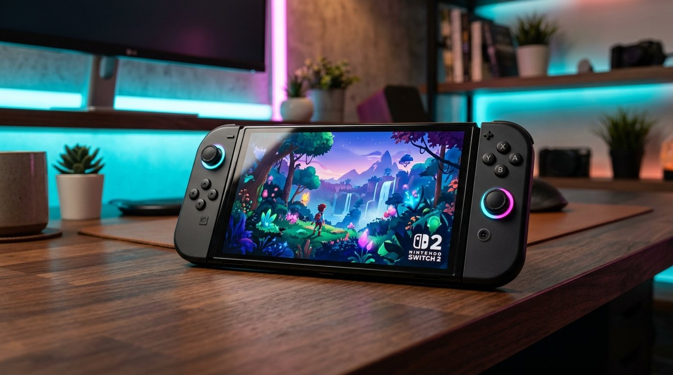
Detailed silicon telemetry and developer SDK documentation have confirmed the hardware architecture powering Nintendo’s next-generation console: the Nintendo Switch 2. Built on a customized Nvidia Tegra T239 SoC (Drake), the hybrid handheld pairs 8 ARM Cortex-A78C CPU cores with an Ampere-derived GPU featuring 1,536 CUDA cores, dedicated RT (Ray Tracing) cores, and 48 Tensor Cores. With 12GB of high-speed LPDDR5X unified memory, the Switch 2 leverages Nvidia DLSS 3.1 to reconstruct internal 1080p–1440p renders into crisp 4K docked output on modern displays.
The Silicon Architecture: Nvidia Tegra T239 Deconstructed
The original 2017 Nintendo Switch operated on an off-the-shelf Nvidia Tegra X1 (Maxwell architecture) manufactured on a 20nm/16nm node, generating a modest 0.39 Teraflops in docked mode. The custom Tegra T239 represents a generational leap spanning four architectural cycles (Maxwell $
ightarrow$ Pascal $
ightarrow$ Turing $
ightarrow$ Ampere).
Fabricated on a refined 8nm/4N process node, the T239 balances power efficiency with sustained graphics throughput. In handheld mode, the SoC operates between 10W and 15W total system draw, delivering visual fidelity on par with a base PlayStation 4 while running on an integrated battery. In docked mode, expanded thermal headroom allows the GPU clock to boost up to 1.15 GHz, generating over 3.1 Teraflops of FP32 compute.
| Hardware Specification | Original Nintendo Switch | Nintendo Switch 2 (Tegra T239) | Generational Multiplier |
|---|---|---|---|
| CPU Architecture | 4x ARM Cortex-A57 @ 1.02 GHz | 8x ARM Cortex-A78C @ 1.80 GHz | ~4.5x Raw IPC Throughput |
| GPU Compute Units | 256 Maxwell CUDA Cores | 1,536 Ampere CUDA Cores | 6.0x Shader Core Density |
| Unified Memory (RAM) | 4GB LPDDR4 (25.6 GB/s) | 12GB LPDDR5X (102.4 GB/s) | 3.0x Capacity / 4.0x Bandwidth |
| AI Upscaling Hardware | None (Bilinear / FSR 1) | 48 Tensor Cores (DLSS 3.1 Support) | Hardware Machine Learning |
| Internal Storage | 32GB / 64GB eMMC 5.1 | 256GB UFS 3.1 High-Speed Flash | Sub-5s Fast-Travel Loading |
The DLSS 3.1 Factor: How 4K Docked Gaming is Achieved
The most revolutionary aspect of the Switch 2 is its integration of Nvidia’s deep learning tensor pipeline. Handheld devices historically face thermal and memory bandwidth bottlenecks when attempting to render native 4K resolutions (3840×2160 pixels).
With DLSS 3.1, developers can render games internally at 1080p (requiring approximately 2 million pixels per frame) while Nvidia’s Tensor Cores evaluate temporal motion vectors and optical flow fields to upscale the final frame to 4K (8.3 million pixels). This allows demanding modern engines—such as Unreal Engine 5 with Nanite geometry—to run smoothly on Nintendo hardware without sacrificing portable battery endurance.
For comparative mobile and handheld silicon analysis, examine our breakdown of Switch 2 Indie World Showcase & Devkit Leaks and review modern display pairing in our Best 1440p 240Hz vs 360Hz Gaming Monitors Guide.
Related posts:
 Nintendo Switch 2 Hardware Deep-Dive: T239 Chip Architecture, DLSS 3.1 Docked 1440p & Battery Lifespan
 Nintendo Switch 2 Magnetic Joy-Con Patent Breakdown: Optical Mouse Sensor & 100% Game Transfer
 Nintendo Switch 2 Hardware Leak & Backward Compatibility Report: NVIDIA DLSS 3.5, Magnetic Joy-Cons & Launch Lineup
 Nintendo Switch 2 & Indie World Showcase Analysis: Tegra T239 Specs, DLSS 3.5 Upscaling Telemetry & Full 2026 Lineup